
The Need for a Clear Guide
Longtime Atarians will remember that as long as the TT has been around, its owners have had to deal with questions as to its revision or version either to satisfy their own curiosity or finding it out for someone helping them troubleshoot it. This seems to affect the TT more than any other Atari model in my opinion. While almost every Atari 16/32bit-system had several revisions of the motherboards, with probably the Mega ST having the most of them, there would never be a shroud of mystery around them. STFM owners who bothered to find out their version probably only needed to know where the CPU was and that was enough for them.
Atari TT always intrigued people, right from the start. Here is why I think we pay so much attention to Atari TT revisions.
It was the fastest machine Atari ever produced.
It was beyond most Atarian's grasp in terms of cost and a dream for many even today.
There were rumours and official documents acknowledging a TTX system that never saw production.
Atari had originally intended the TT to be a 16MHz unit and at the last minute decided to go with 32MHz and implementing a solution that doubled the CPU clock while keeping the bus at the original 16MHz. This implementation is what we know as the daughter-board.
Some 16MHz units were sold to the public causing owners, especially 2nd-hand owners, to want to know if they were unfortunate enough to end up with one.
As years went by Atarians started to notice that TT motherboards changed and with Atari's very confusing versioning, all kinds of naming standards were created by users that probably had no base in reality. I myself have adopted Simbo's style as, love him or hate him (I wish he was around), he was one of the leading TT-experts. However, as I have gone deeper and deeper into this rabbit hole, I've come to realize that this may not be the most accurate naming scheme after all.
At this point, we need to clarify and recognize a few facts about Atari's versioning system and how they themselves refer to the different motherboard models. There are industry standards to PCB manufacturing at this scale. I won't pretend to be an expert, in fact, I know jack squat. I do know that there are FAB (fabrication), and ASSY (assembly) numbers and Atari used them typically in every system.
Cybercube's CaTTamaran installation guide offers some clues to identifying the various revisions but they seem to have yet another system of classifying revisions. They were, however, a very reputable company developing cutting edge TT030 specific hardware so we need to assume that they knew what they were talking about and probably saw and handled more TT's than most others. So we'll look at their instructions as well.
Explanation of Terminology
First, we need to establish the TT lingo and help any newcomer to come to grips with the terminology that will get thrown in this guide. In no particular order:
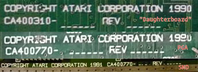
SMD: Used to describe the latest model motherboard (surface mount device)
PGA: Used to describe the middle model with socketed CPU (pin grid array)
Daughter-board: A small PCB used on the earliest model that contained the CPU and circuitry to run the TT at 32MHz
Silkscreen: The (usually) white writing on PCBs used to denote components, revisions etc.
Rework: Hardware patch issued by Atari to upgrade system to a higher revision.
ECO: Engineering Change Order, same as rework
ASSY: Assembly. Atari always uses CAxxxxxxxx
Here are three versioning schemes typically found on the Atari TT:
1. The Silkscreen Revision (ASSY #)
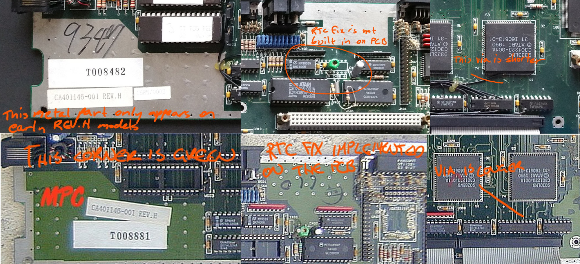
This is the revision most of us are most familiar with. It appears on every single TT motherboard. Unfortunately, this is also the least accurate identification method since that number did not change at all since the early PGA (non-daughterboard) model. Only the very first model can be identified by it but still, it contains several revisions within it. Pictured below is how it appears in the various models.
Cybercube implies below, that some boards have had some handwritten REV numbers added later, perhaps after a rework procedure. I've heard of some reporting what looks to be a smudged letter but illegible.
= INSTALLATION STEP 1 =
Check the motherboard revision of your
system:
You can usually find the revision printed on
a white label in the lower right hand or
left hand corner of the board. If your board
does not have one of these stickers, check
the REV ___ field as shown. If the revision
field is blank, check if the CPU (MC68030)
is situated on, the right side of the board.
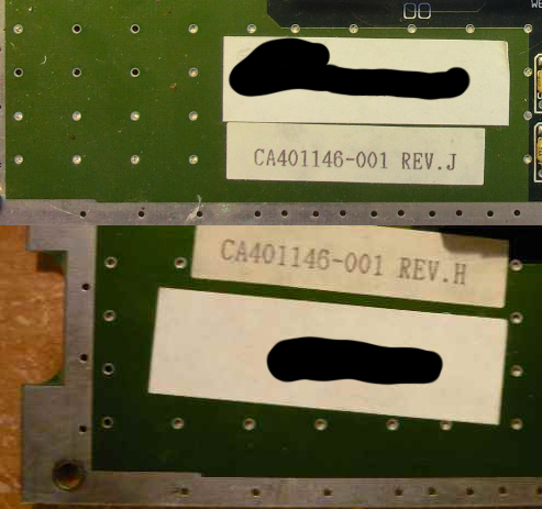
2. The Sticker Revision (Also ASSY #)
This sticker appeared on the bottom left corner of the component side of the board in the SMD models. Earlier FABs did not have that sticker unless authorized Atari servicemen performed the rework procedures that upgraded the system and added the sticker. More on that further below. Since this method only applies to later models and doesn't tell the whole truth, this is only a semi-accurate but quick way of trying to identify your TT. Pictured below are a couple of examples.
Another excerpt from Cybercube:
/// How can I find out if I can install a CyReL CaTTamaran in my TT?
==================================================
That depends mostly on your TT030 motherboard revision. To establish
which TT030 motherboard revision you have, you must open your TT030.
Please note that this may void your warranty. Once you removed the
cover (and any metal shielding), please check the lower lefthand or
righthand corner of your motherboard. Write down the revision level
usually found on a white sticker on the motherboard. For a quick and
easy installation, you should have at least REV. G.
I personally have never seen boards that have stickers from D-G. Keep in mind, Cybercube was a Canadian company and Simbo once theorized that perhaps the TT revisions vary regionally for whatever reason. He had observed, after servicing numerous TTs in Scotland, that the boards he typically got were from Europeans and the SMD models were usually stickered H,J, or K. Something to keep in mind. Again, if anyone has pictures of these boards, please email them to me.
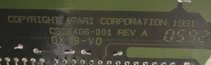
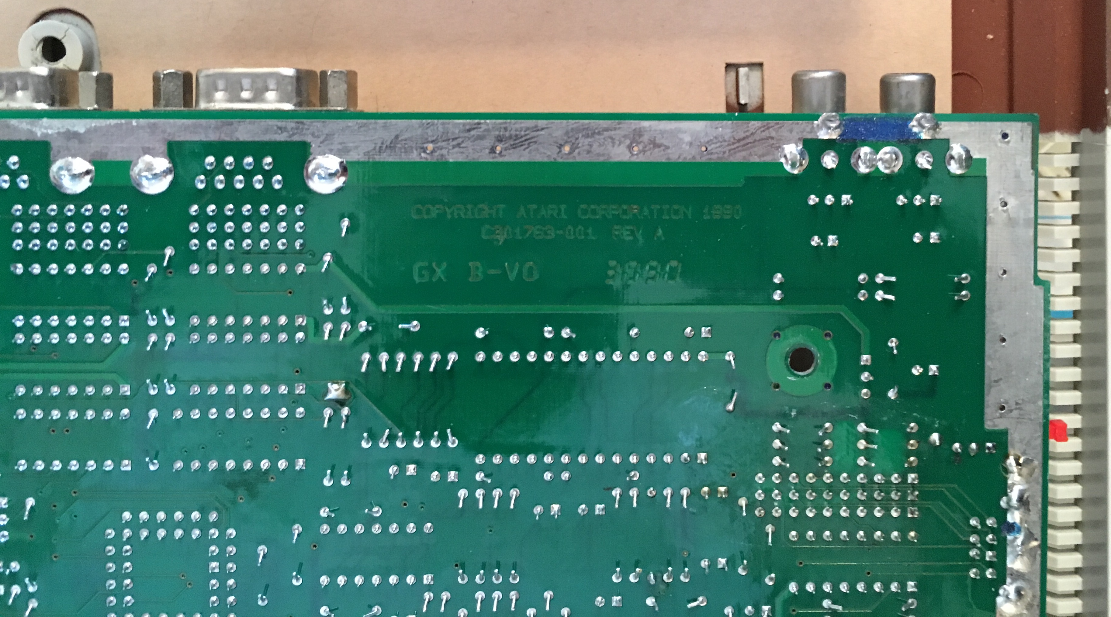
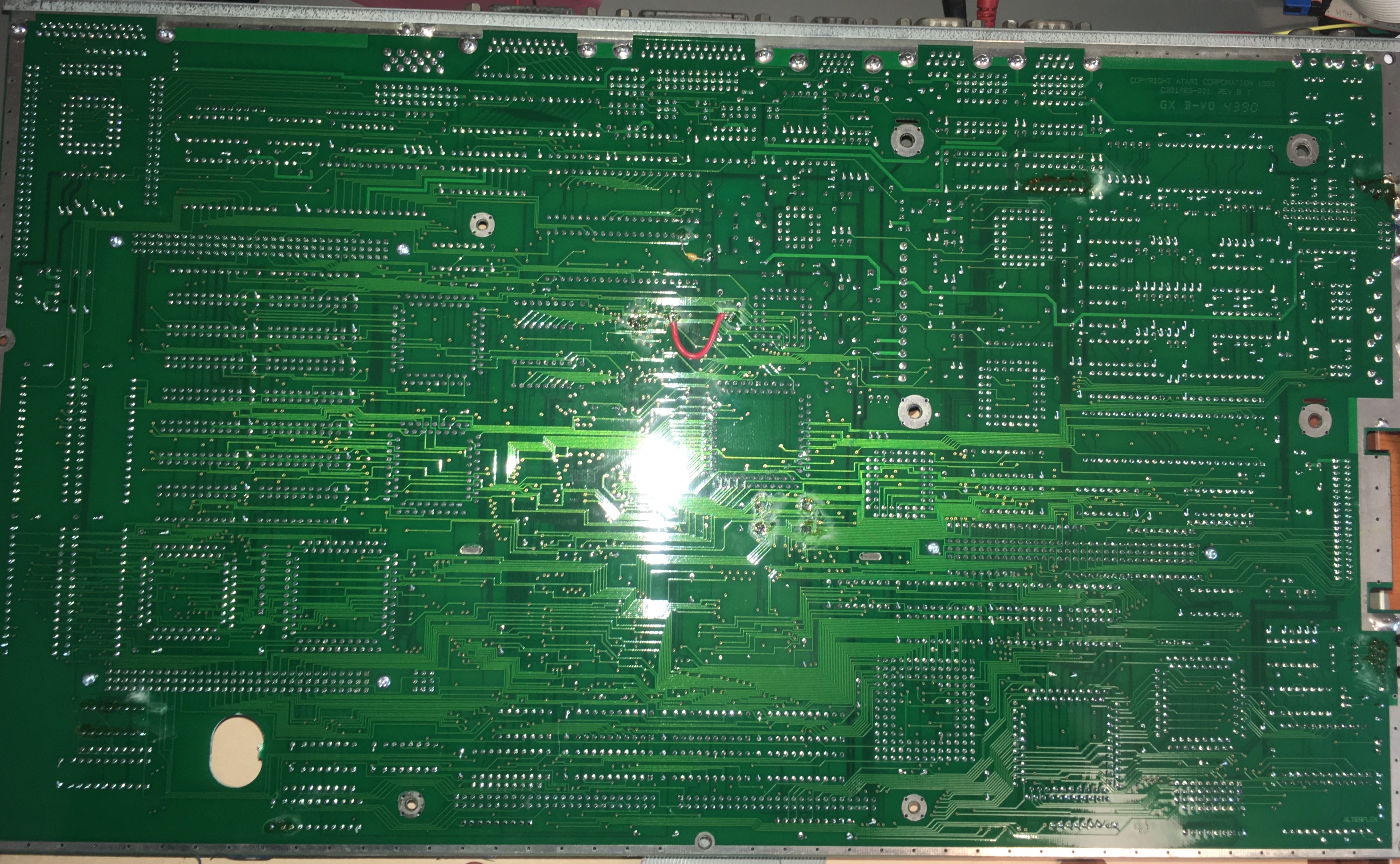
3. The Fabrication Number
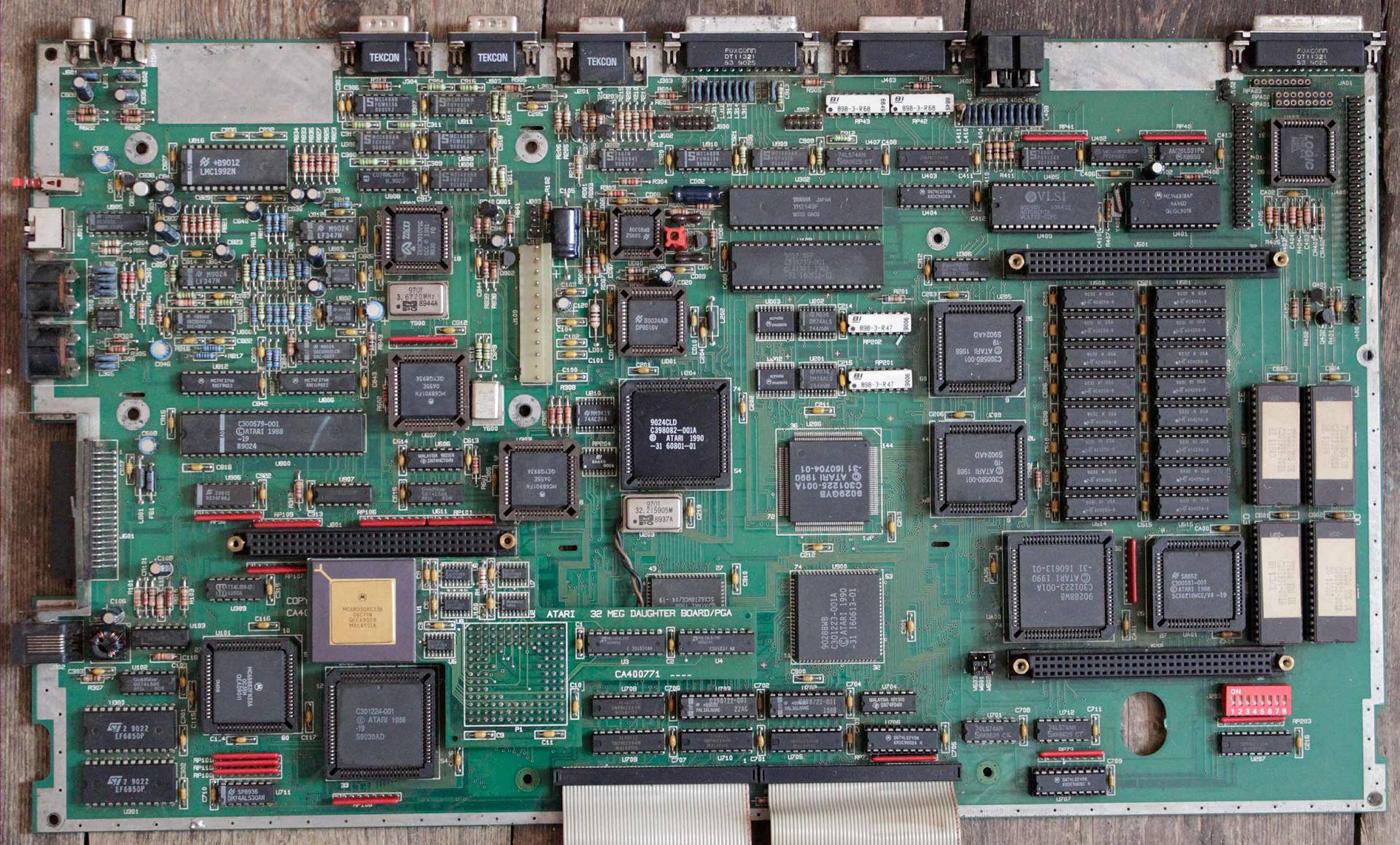
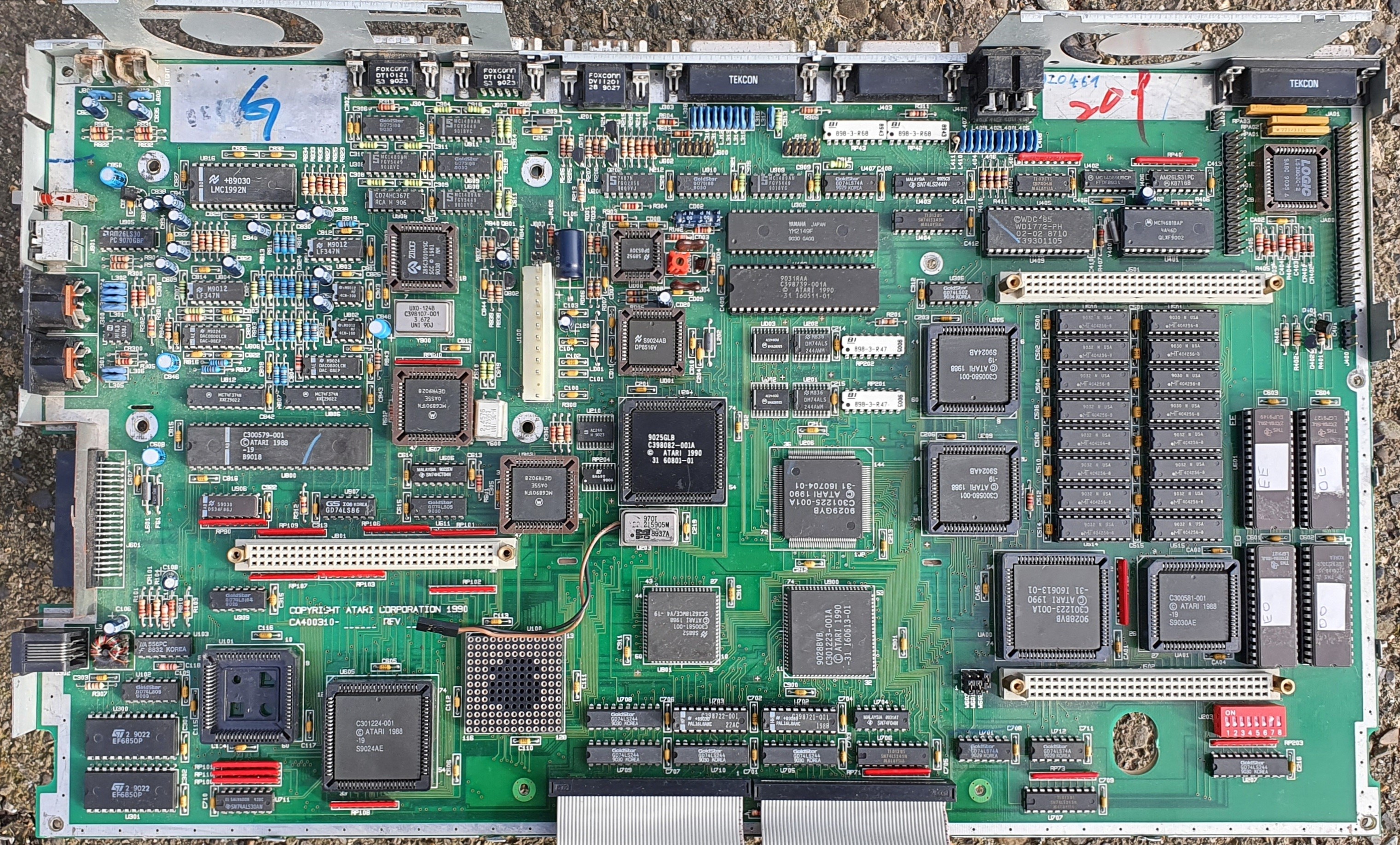
This is the only way of accurately determining the exact board revision (FAB) down to it's sub-revision (REV). Consequently you get the manufacture date from the same location giving you the week# and year (WWYY). It appears on every TT motherboard without exception. Unfortunately, this information is located inconveniently on the solder side (back side) on the edge of the motherboard where the rear connectors are. You would need to strip your TT completely just to get its revision number. I believe this to partly be the cause of the problem we have. We either are not aware of its existence or we don't want to (understandably) go through the risky process of dismantling the TT just to satisfy our curiosity. Pictured below is an example of this number and associated information.
The Absurdity of the Revisions
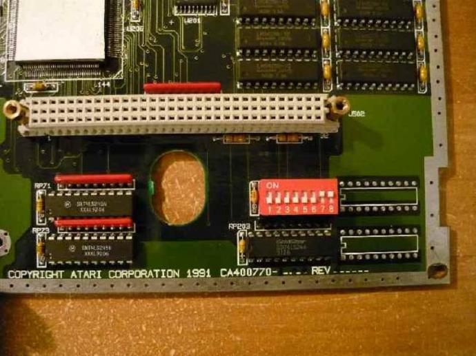
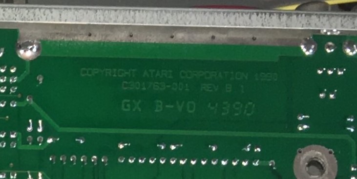
Here is a typical example of what we commonly call REV.H. All these can be found on same the PCB:
CA400770 (Silkscreen - CA# are always ASSY)
CA401146-001 REV.H (Sticker - ASSY)
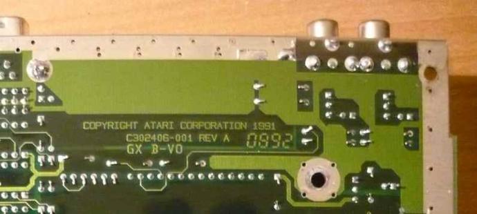
C302406-001 REV A (FAB & REV)
The following pictures are of the same board depicting these numbers.
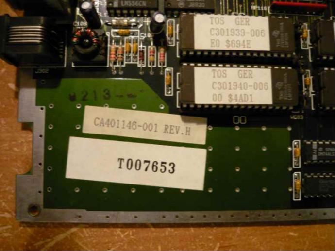
So it's a REV.H and a REV A? My PGA model is REV A as well but most are B1. But we call the PGA models REV.C! WTF?!
Do you now understand my primal urge to sort this once and for all?
Atari's Usage of Revisions
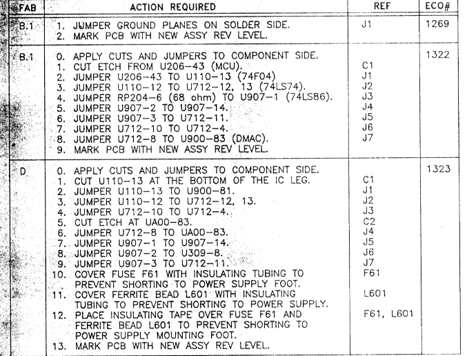
We, fortunately, have plenty of material that shows us Atari using a fairly consistent naming scheme. On internal documents such as rework guides, ECOs, and schematics Atari either used the full FAB number from the back or the last letters of that same number as shown below.
Here is another one.
Notice how Atari distinguishes REV from FAB?
For public documents, we have an example below from the Atari System V release notes listing specific compatible revisions by the same FAB & REV combination.
However, I have not found documents where Atari is referring to the very first models by some revision number. All the rework procedures are for either B1 (or B.1) or D. And clearly, B1 is the PGA model and D is the latest SMD model. And we know this for a fact as Atari included pictures of component placements for both revisions. But that only covers only two REV examples of the same FAB, or does it? Does this mean that the patches can't be installed on earlier than B1 revisions? But I successfully installed them on a REV A. Does it mean that later revisions from D don't need the patches? More on that later.
So I believe, from the evidence above, that the only way to accurately identify and communicate the TT revision is by following Atari's example of using the FAB & REV combination from the underside of the board. And this would be the end of this guide if it only were that easy. Since it is a massive undertaking for anyone to go through the process of dismantling the TT, there has got to be another easier way.
Already at this point, I have to concede that we will have to continue to use our various ways of communicating the different revisions. And I'm totally fine with that. The point of this guide is to bring everyone to the same page. Give visual aids to help identify the board. And when the FAB & REV info is not available, use some other combination of facts to narrow it down very closely.
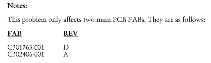
The Three Atari TT030 Motherboard FABs
Wait, what? Three? Surely there are more. Well, these are FABs and they have REVs. This is a logical conclusion and please prove me wrong if you can. But I believe Atari only had three major TT board FABs.
C300720-001 and its various REVs
C301763-001 and its various REVs
C302406-001 REV A
Don't worry about the other ASSY numbers. They are irrelevant but we can use their position on the board to help identify the different revisions. The REV.# on the sticker after the ASSY # is helpful but can be misleading as I'll show later.
So let's break down each of the three FABs and try to drill into their REVs.
C300720-001
What We Know
This is the very first TT motherboard FAB.
This board was not designed for 32MHz, hence the daughter-board that plugs into the CPU socket.
As the only FAB that can be identified by the ASSY#, it's ironically hidden under the daughter-board. But the daughter-board in itself is enough to identify the board as FAB C300720-001.
Other than the PALs and other circuitry that the subsequent FAB had, it appears that the rest of the board layout is pretty much identical.
If your TT has two fans at the back, you most likely have this FAB.
Almost certainly you have metal shielding in your case.
So what REVs are within this FAB? I will provide evidence that each of the three FABs had a REV A. So there's that at least. Chips 'n Chips only lists a REV 5 for this FAB for both the 16MHz and 32MHz PGA. I have never seen this REV mentioned or referenced elsewhere. I have only seen REV A and B.
REV A
It's bad quality but I assure you it's a C300720-001 REV A. So if this REV A has a daughter-board, maybe the REV 5 is the earlier 16MHz model? Could be, but according to this post, Eddy, who was one of the TT owners questioning his TT's performance, provides us with a very detailed description of his board.
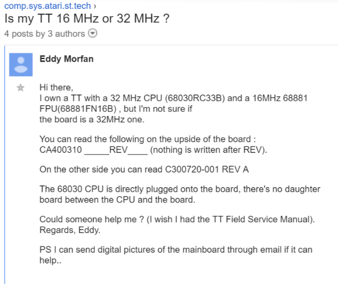
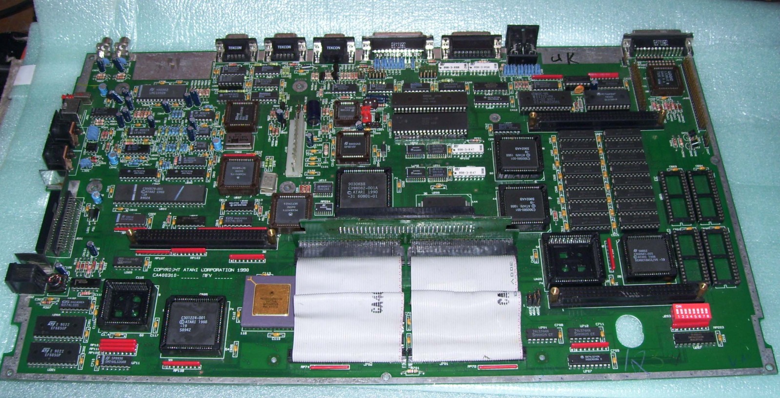
This leaves no question then. His is a REV A, 16MHz unit as there is no way this particular FAB can be 32MHz without the daughterboard. So what does a TT without the daughter-board look like? Take a look below:
**UPDATE** REV B
I have been approached by Michael Farrell, who recently bought a non-working TT that turned out to be a C300720-001 REV B. He has kindly provided pictures for us. Note that his is a daughterboard model with it removed.
What No Longer is Unclear
Now that a REV B has surfaced, we no longer have to speculate about other revisions in this FAB. At this time I would like to discuss one issue relating to our current naming standard where A-C are the daughter-board and PGA models and D-K are the SMD models. We can safely assume that if REV A is in fact C300720-001 REV A and REV C is the PGA model we will talk about next, where does that leave REV B?
According to Simbo's post in Atari-Forum:
then rev b was the same but had a better clock setup
and you can by this time add the 32mhz mpu daughter board it has the pal ics added to it
and here:
rev A had the mpu onboard gold top and you could add a daughter board to its socket and it was 32mhz instead of 16
So not sure what to make of this. Simbo is basically saying REV B does not exist and has mentioned elsewhere that he has never seen one. We now have evidence of REV B's existence but it still could be that it never made it to market, at least in large quantities. Cybercube, on the other hand, speak of REV B as what we call PGA or REV C. They don't acknowledge a REV C at all.
Schematics
I have enhanced the schematics and can be found here: Schematics
There are only two different schematics available for the TT despite there being all kinds of seemingly different versions. There is Revision 1, which is the one above and mistakenly referred to as Revision I. The other one is Revision G. That's it, that's all.
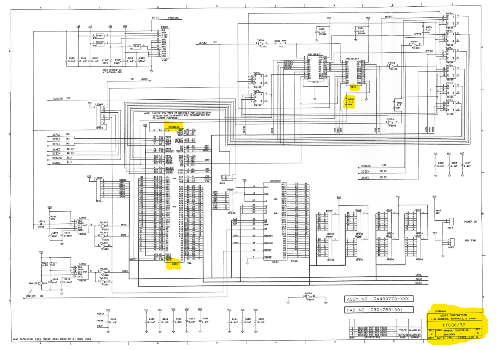
How do I know this is Revision 1 and therefore precedes Revision G? Simple. I've explained it on the schematic but I will illustrate it here. C300720-001 and C301763-001 REV A-B1 have components that don't exist in later models such as the RP42. And likewise, C301763-001 REV D and later have components that do not exist on the early models like the R888. Let's look at both:
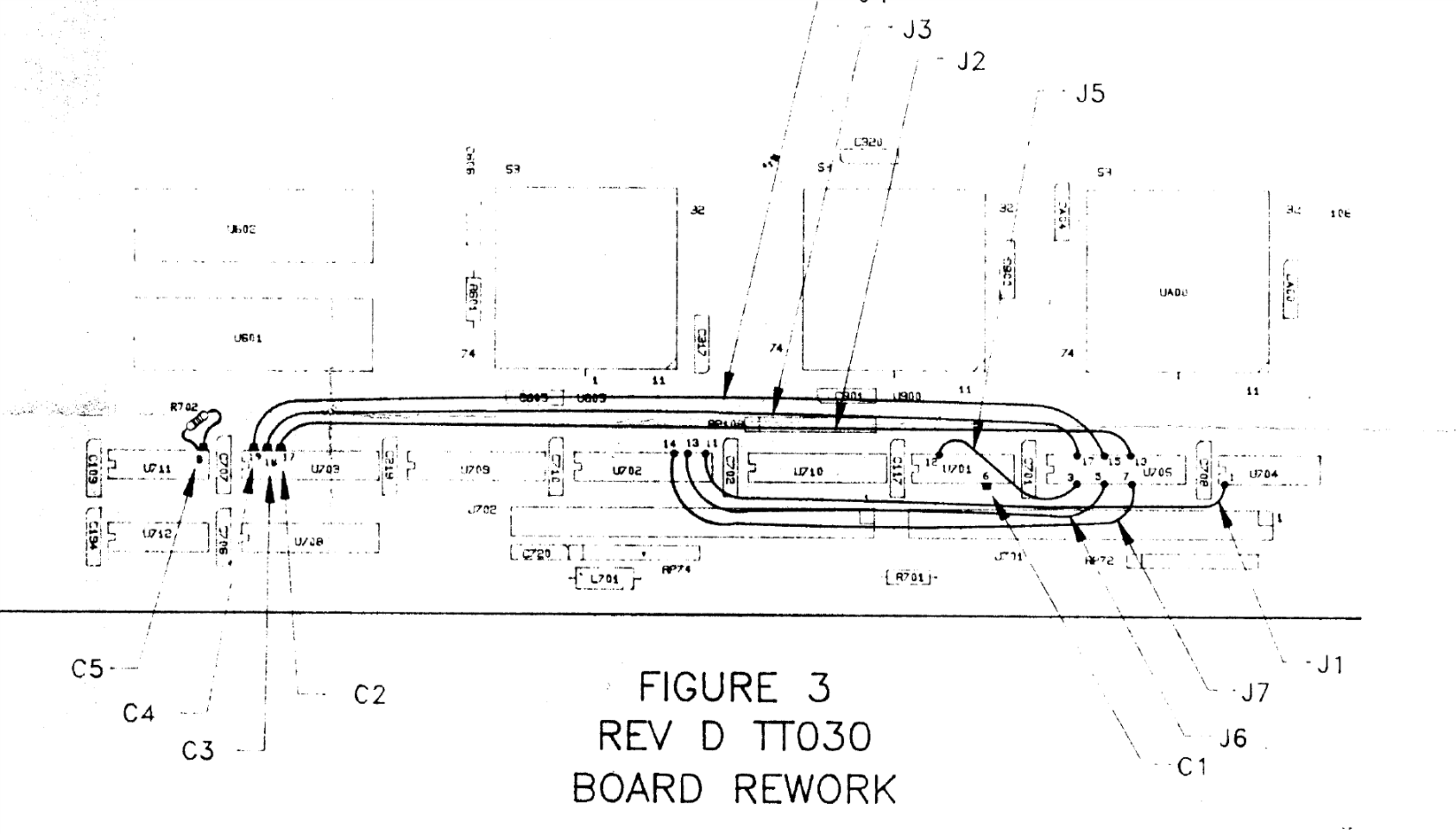
I chose RP42 as it was a B1-only rework. Here it appears on Revision 1:
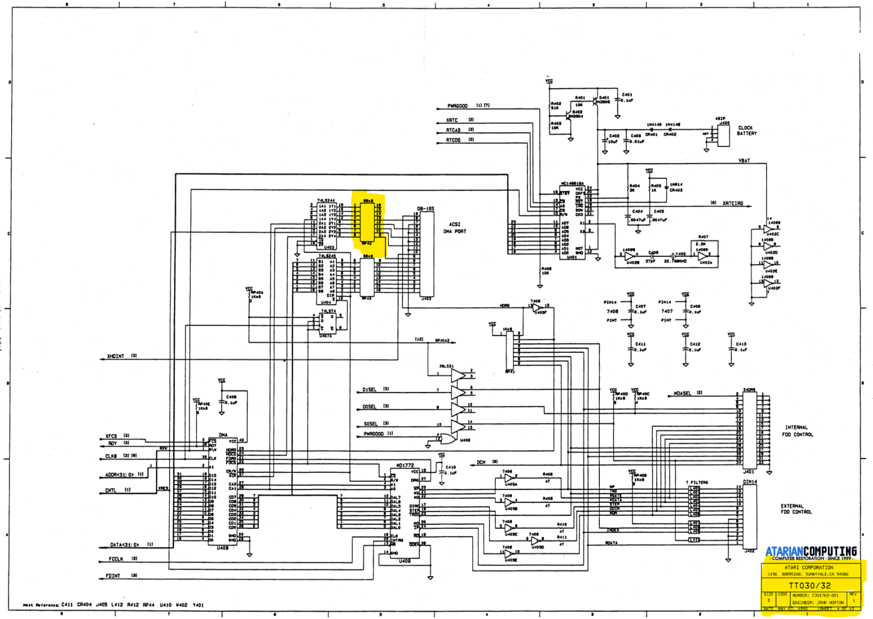
And RP42 not in Revision G. Just single resistors just like on the board itself:
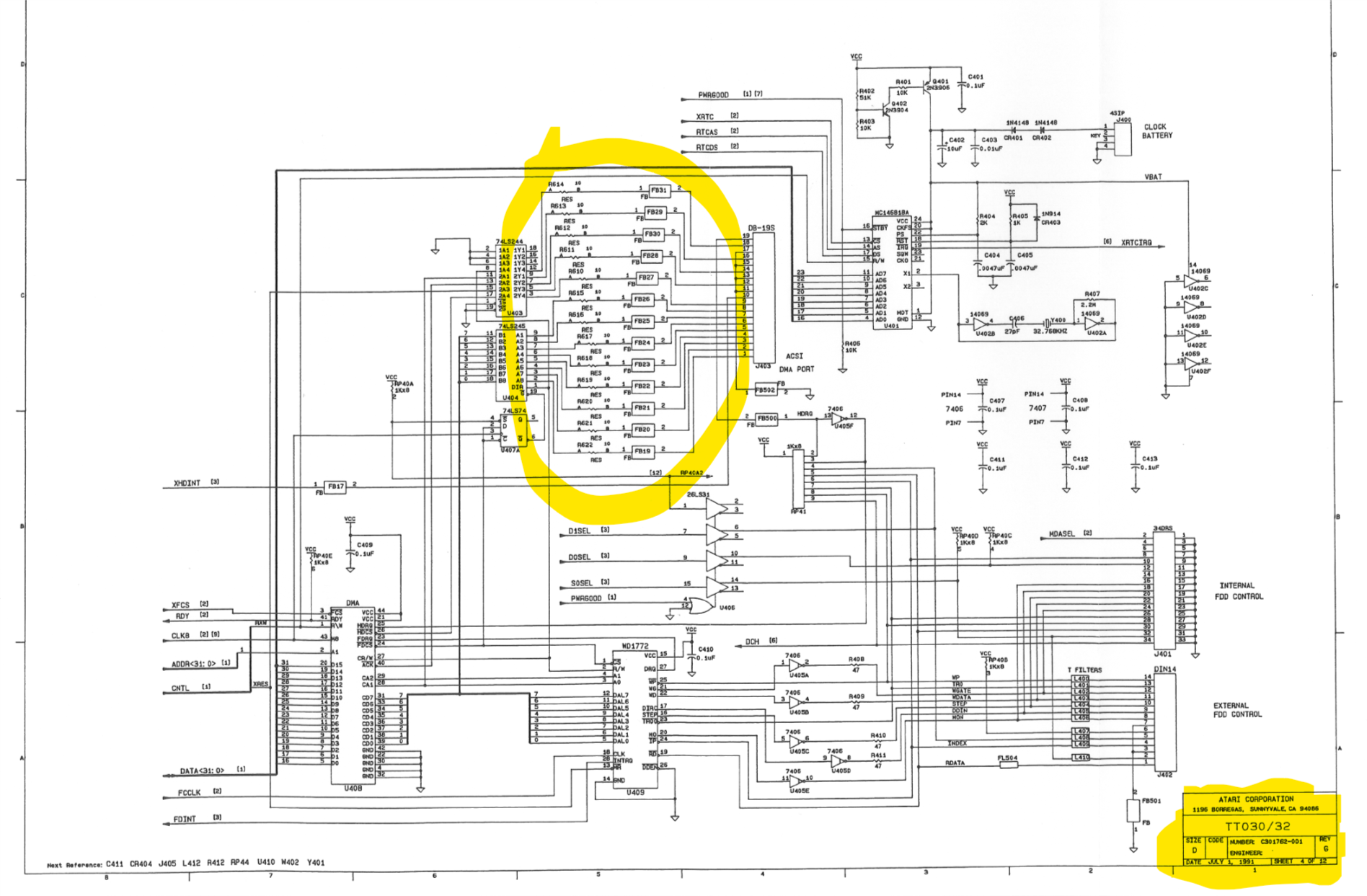
Then we have the small R888 I chose because it plays a big part in reworks meant only for SMD models and CaTTamaran installation for SMD models. Here it is on Sheet 1 of Revision G:
And here it isn't on Revision 1 as it does not exist on the board:
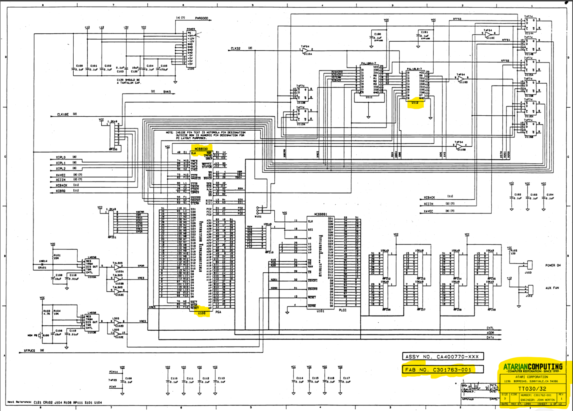
Note that I highlighted the FAB C301763-001. This is further proof that the C300720-001 is very similar to the C301763-001. This schematic includes the daughterboard schematics so clearly meant to be used for that model. Also, this schematic refers to REV D at times so this is a relatively late schematic for being our earliest.
Conclusion
Despite some seemingly contradicting information, this FAB remains perhaps the easiest to identify and communicate. I suggest that going forward we use any of the following to communicate this particular model:
Daughterboard model
REV.A or REV.B in conjunction with another clarifying term
First Revision
CA400310
C300720-001 REV *
C301763-001
REV A
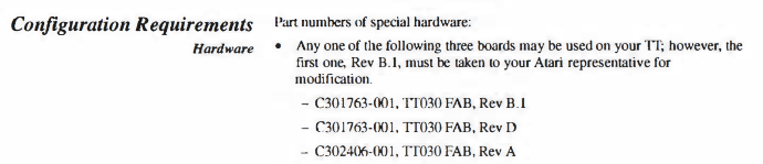
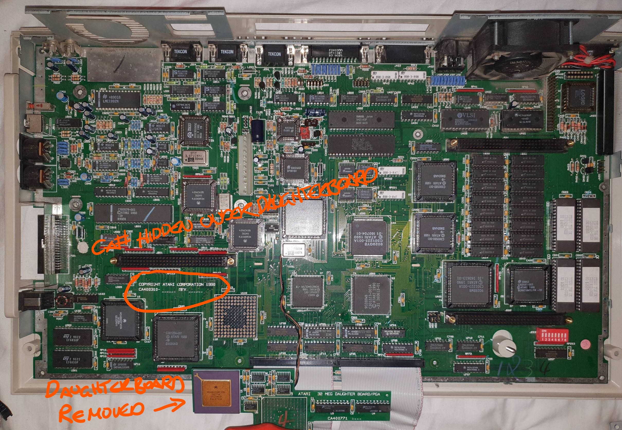
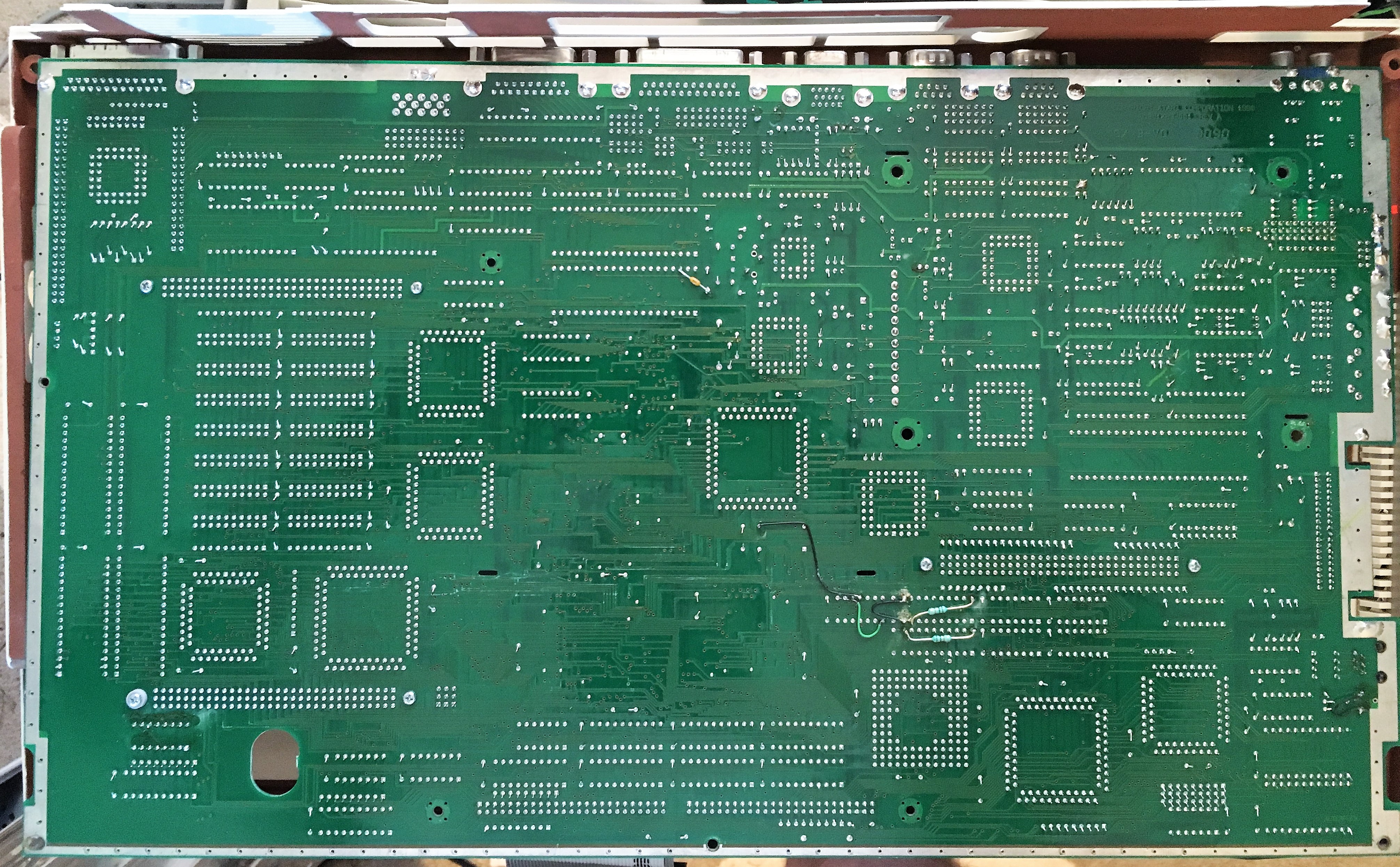
Although we usually hear and read of REVs B1 and D in this series, logically there has to be a REV A. My current TT happens to be one. Here are pictures of it prior to any mods.
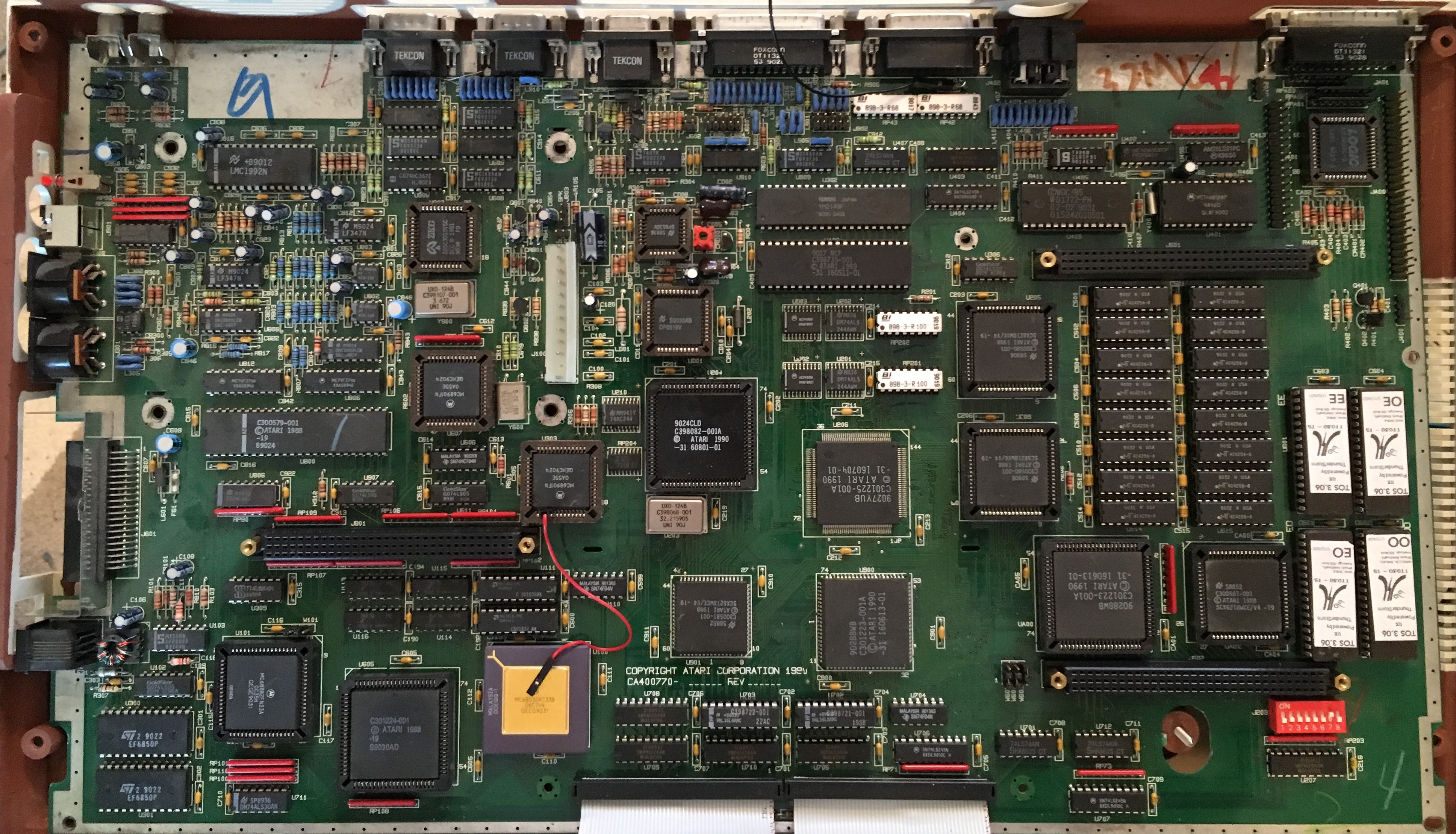
Notice how the daughterboard circuitry is now located between the CPU and the TT-RAM connector? That's where the ASSY# was located in the C300720-001 FAB and that designation has moved to right above the VME circuitry. This is one way of telling the two FABs apart.
I was surprised to find out I had, what perhaps is the first model of this FAB. Obviously one starts to think of what crucial change, that spawned REV B1, is missing from this board? Is it the rework shown above on the solder side? I've cleaned it up since by the way. So I don't know what to think of this.
I have very successfully made all the patches according to my Atari TT030 REV.C Rework Guide and outlined here: My TT Gets Some Love. Even though they were meant for B1. I have never had issues with this model. All upgrades (Thunder, Storm, Lightning, NetUSBee, Nova Mach64, ECL2VGA, PicoPSU, Parcp-USB) have performed flawlessly. The same could not be said of my previous B1 model. Thunder never worked on it, all kinds of weird issues. I actually bought this TT to replace that because of these issues I didn't want to deal with at the time.
REV B1
This is the revision we think of when we talk about the PGA model. Here are pictures of my previous TT:
Please excuse the glare from the flash. Visually no discernible differences between A and B1 that I can see. Manufacture dates are within four weeks of each other.
One immediate question comes to mind; where is REV B? I assume that as REV B was about to go into production some last-minute changes were done that warranted the B1 designation and REV Bs were never manufactured. However, with other models, both revisions have been produced like Mega ST C103544-001 REV 1 & REV 1.1.
REV D
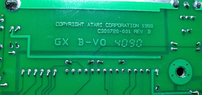
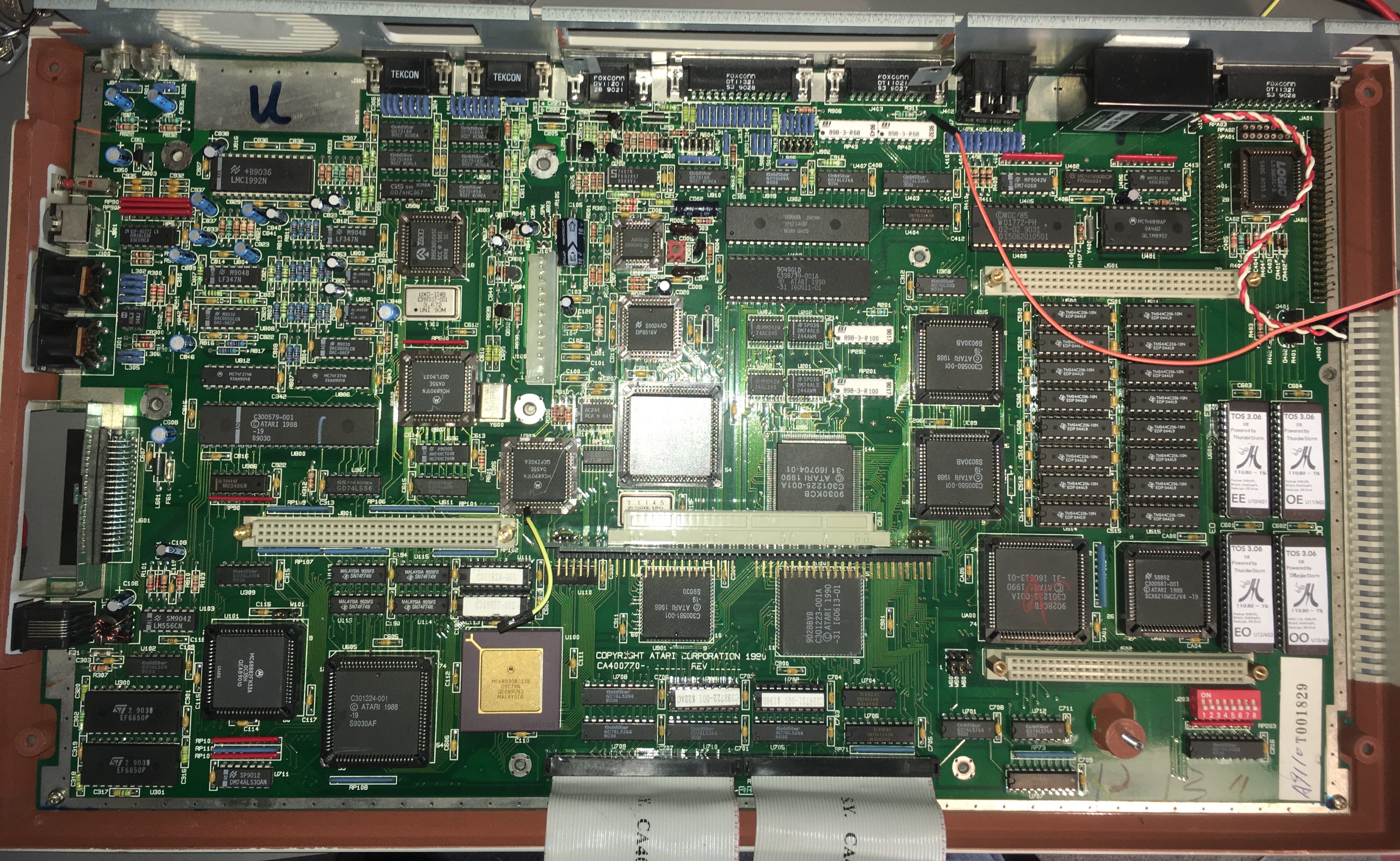
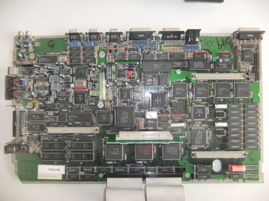
Now comes the part where you will think I have gone nuts. I am including an SMD model in the same FAB as the PGA revision. This is the educated assumption part but I have good reasons to do it and I will provide compelling arguments for it. First, we look at a picture of what I believe is a C301763-001 REV D.
It has no distinguishing markings telling us it's a REV D other than being an SMD model. Here's another board I believe to be a REV D:
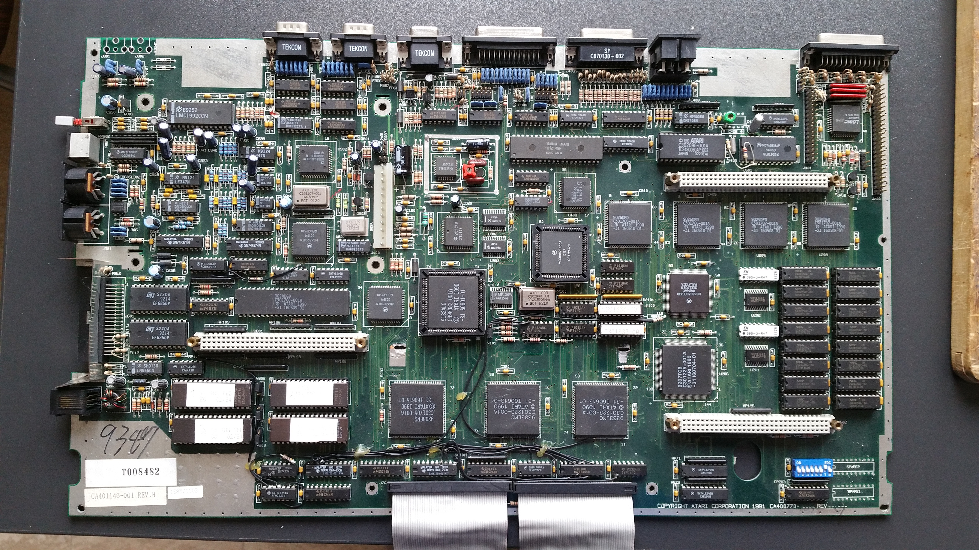
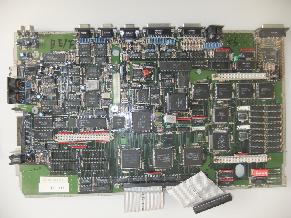
Yes, that's right. It says REV.H on the sticker. But, I believe, that if you were to turn this board around it would say C301763-001 REV D on the back instead of the C302406-001 REV A we saw on a REV.H earlier. I know this overlaps with the next FAB but it's important to set the record straight at this point. Here is a board view of a REV.H on a C302406-001 REV A FAB.
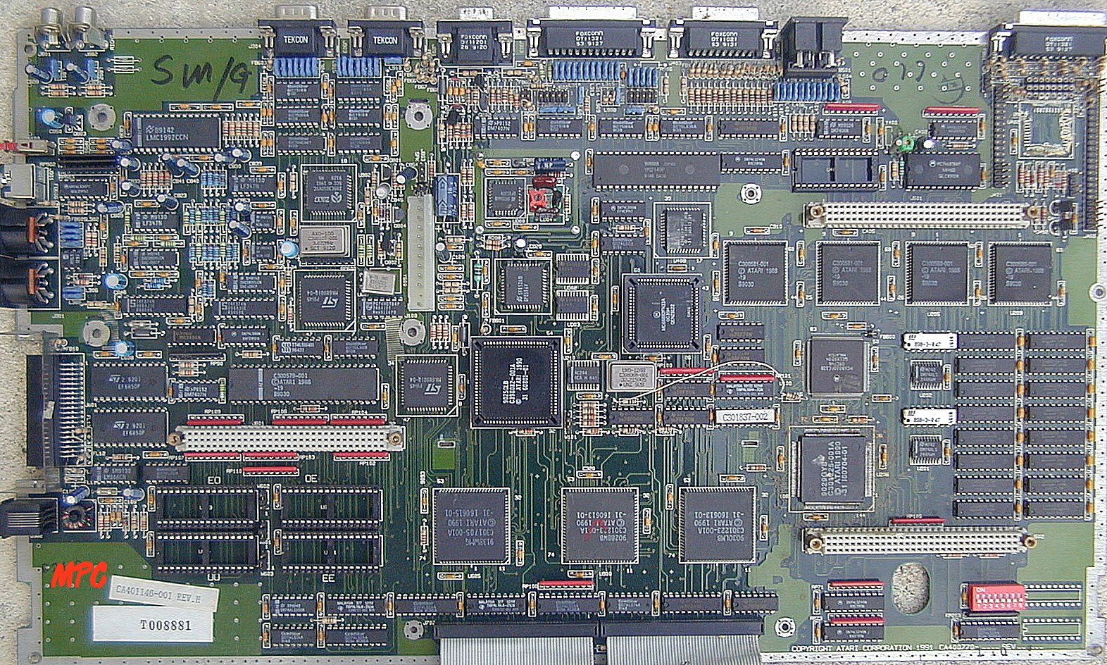
Let's look at key differences.
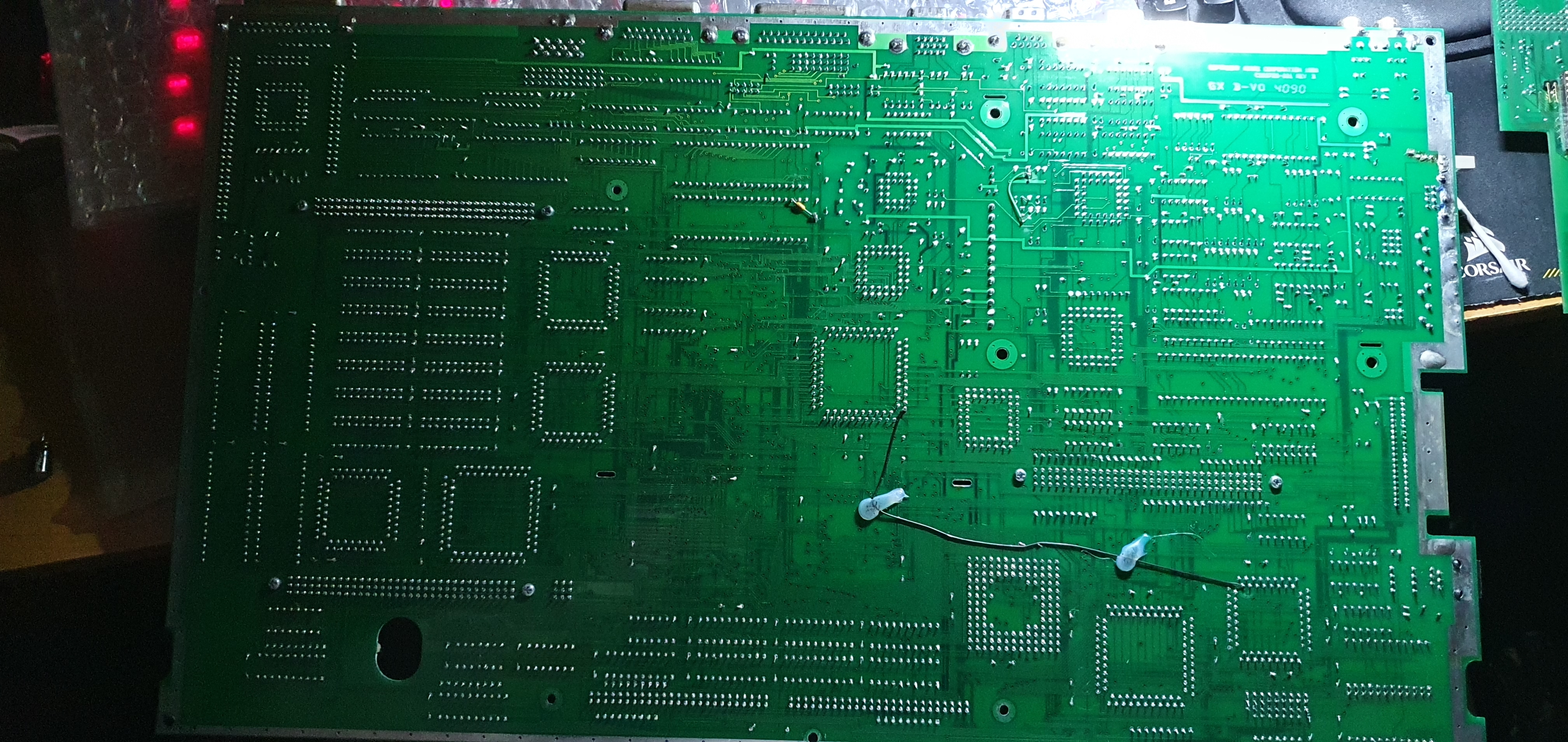
The REV.H on the bottom looks greener where the top one has metal-plated areas and a darker overall appearance.
The top one has wires on the board which seem to be all of Atari's known rework procedures whereas the bottom one only has one next to the CPU.
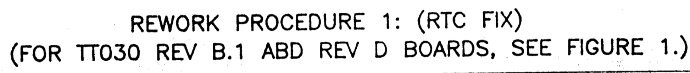
The top board clearly has the RTC Fix done to it by removing U402 as per Atari TT030 REV.D Rework Guide.
The bottom board has never had a U402 so the RTC fix is part of the C302406-001 FAB
This picture will help visualize:
Arguments and Evidence
Here come the compelling arguments as to why I believe the above to be true:
Atari's documents I posted show that REV B1 and D are part of the same C301763-001 FAB
We know that REV B1 and D are PGA and SMD models from Atari's diagrams in their rework guide
REV B1 and D are very similar to each other but just have a different layout.
There are no non-metal plated REV.H or higher with the patch wires we always see on metal-plated REV.H
Atari instructed the ASSY # and revision to be marked after the rework procedure
After rework, the board essentially was upgraded to a higher revision, which is why our example C301763-001 REV D above can be a REV.H at the same time.
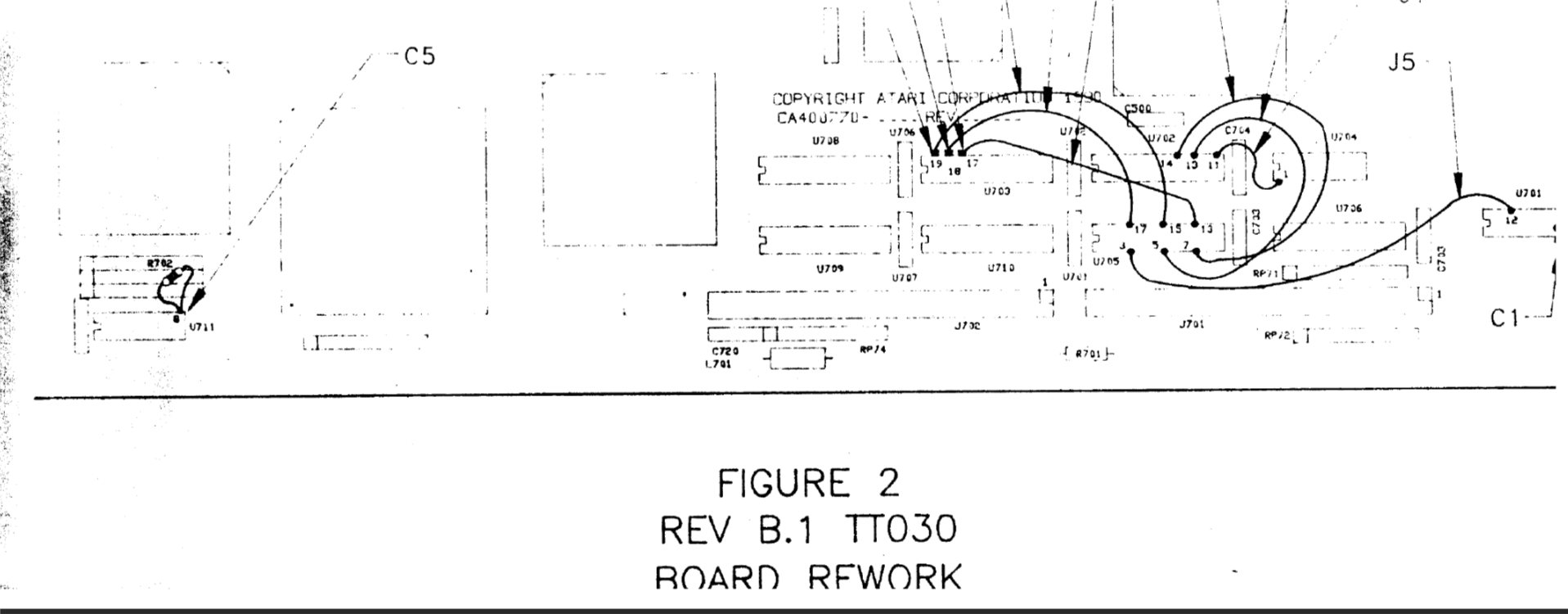
Now I'm going to take out the big guns. Have a look at this sheet:
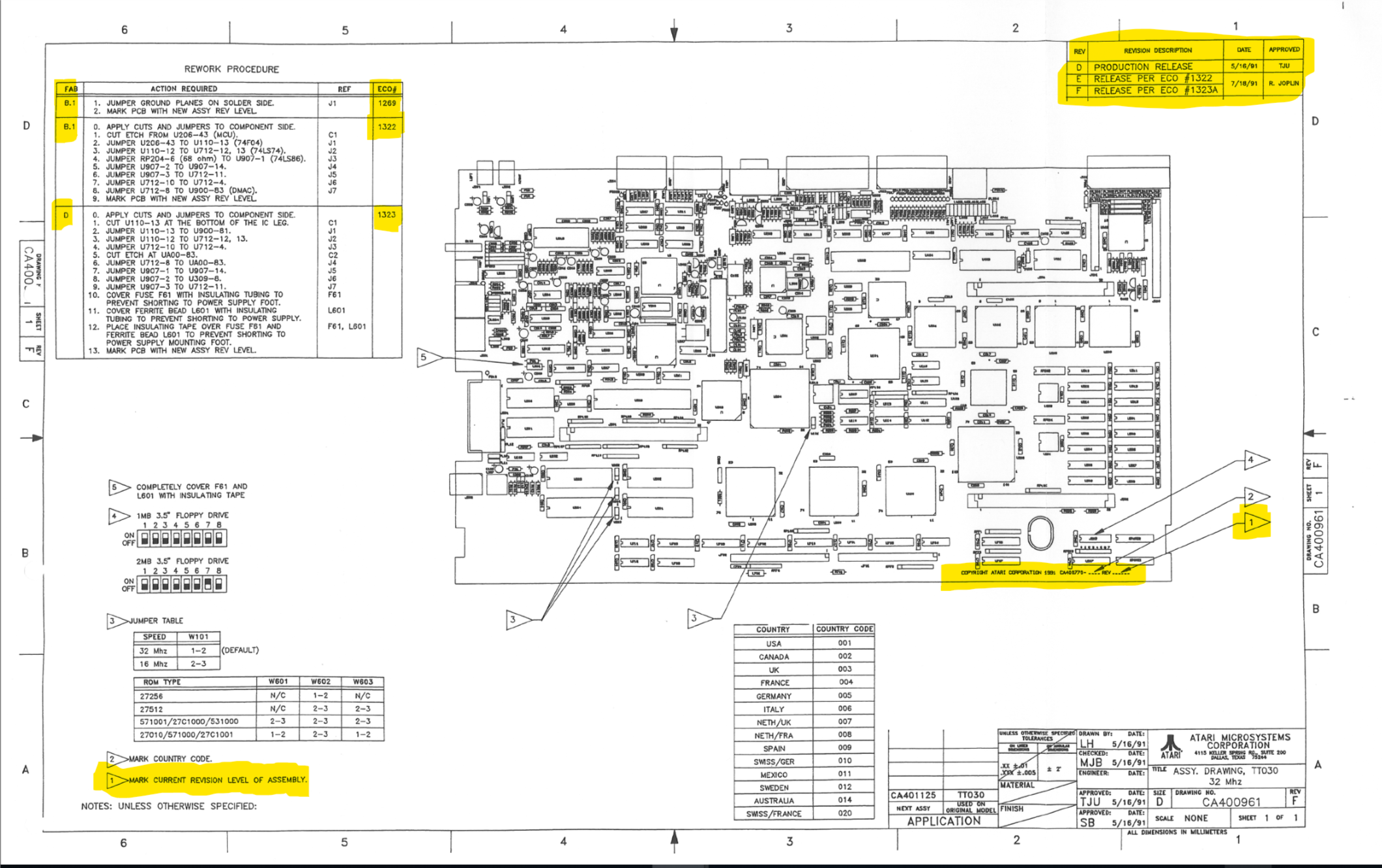
We have here a board view of what clearly is meant to be a REV F. The top right shows the steps to get to REV F. Most important clue here is that REV D is the production release. This can be understood to mean that there weren't separate FABs for each revision. That would be ridiculous. So the base board to apply the patches was either C301763-001 REV B1 or REV D and then mark the revision on the board. The ASSY would be CA400961 compared to REV.H CA401146.
I think that Atari first marked the revisions as described above. This would confirm Cybercube's instructions. But apparently, as reported by users, the mark got smudged and became illegible. Atari at some point, I believe in the beginning of 1992, began using stickers on the bottom half starting with REV.H.
Another interesting observation is also on the top right corner. To get to REV E you would have to perform ECO# 1322 on the board. Look at the rework procedure on the top left. ECO# 1322 is only listed for REV B1, our PGA model. REV F on the other hand is ECO# 1323 meant for REV D. I firmly believe that both reworks are the same thing for different boards which leads to some interesting conclusions:
REV E & REV F are the same revisions but on different board layouts?
There is no SMD model REV E or PGA model REV F?
But forget that because there is this:
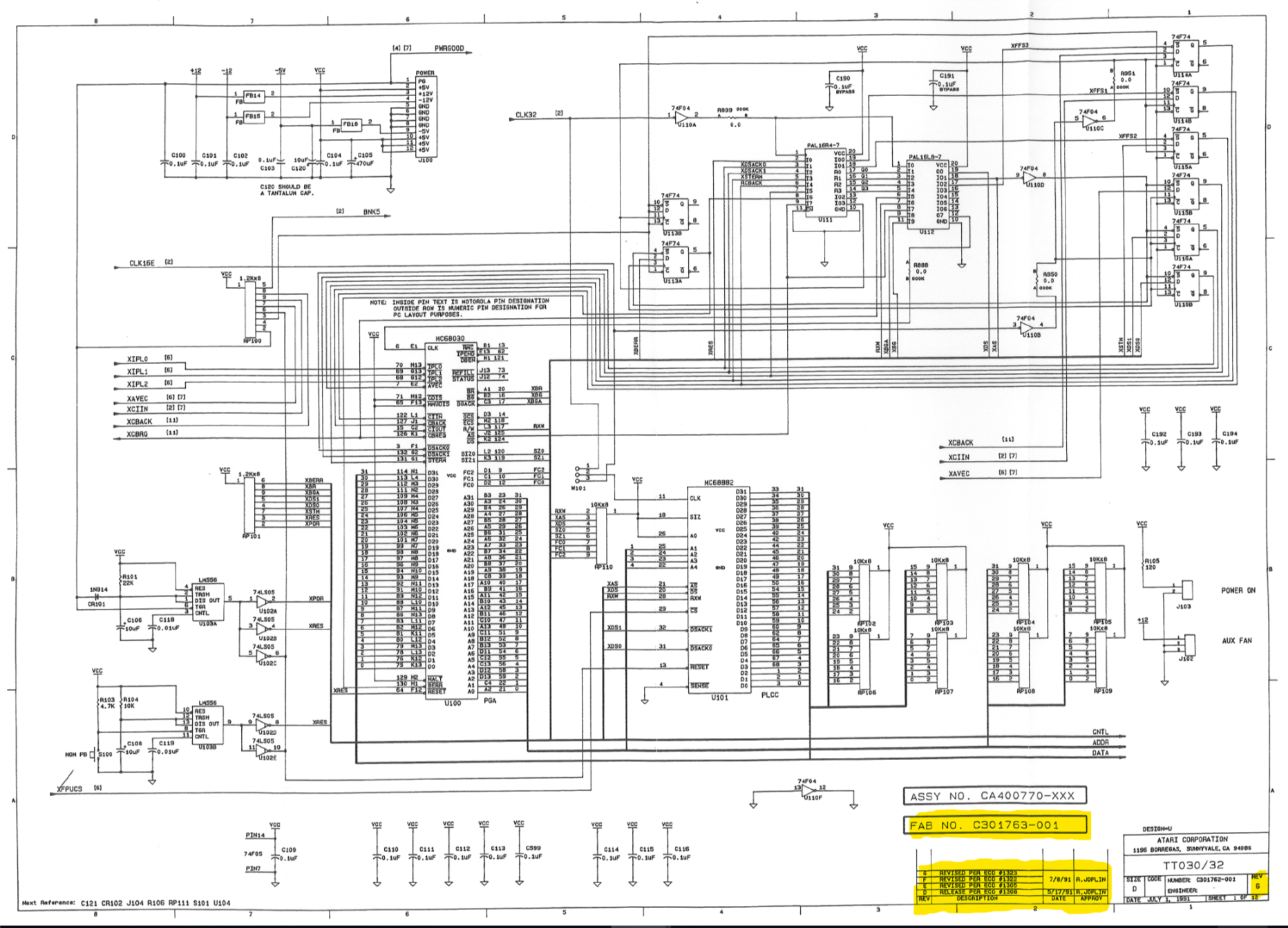
This is Sheet 1 of the latest schematics known to exist. More on that in the next segment. Notice that the board revision is now G. Also note that this is still FAB C301763-001. Notice also that there are steps to get to REV G. But something is not right. REV D now has an ECO# for it, 1308. I do not have information about that procedure. But look at the rest of the REVs. They have different ECOs from the previous ones. Also, now they read Revised per ECO instead of Release. So in the less than two months between these two sheets, there were further revisions.
Let's try to figure out the rest of the REVs.
REV E
The ECO got changed for this REV. We don't have information about 1305. Seeing that this ECO precedes ECO# 1308 for REV D, we could assume that it still only applies to the PGA model REV B1.
REV F
Interestingly this is the same ECO# 1322 as the REV E had earlier. Meaning that REV F is in fact only for the PGA REV B1 and therefore there probably is no SMD REV F in existence. That is unless they managed to mark a few PCBs in the less than two month period.
REV G
The last of the C301763-001 FAB. I mean it has to be. Otherwise, we wouldn't see REV.H on C302406-001 FABs as we clearly do. This also is the same as the previous REV F. Atari apparently nudged a rework procedure in the middle and bumped REVs E & F to F & G.
Schematics
REV A and B1 use the same schematic as detailed in the previous section. Download here: Schematics
For REV D & G you will want to consult the REV G schematic found on dev-docs.org.
Conclusion
This is a lot of information to handle and condense. As to what we should call this FAB, we have to go by several names as there are two significant board layouts for this FAB.
REV A & B1
I think we can continue to call these boards REV.C or PGA
Those names don't conflict with other naming schemes
These names are already well established in the community
Using REV E or F is not recommended unless there is sufficient evidence and you are prepared to explain a lot.
My REV A has all available rework done to it and exceeds REV F by far.
REV D-G
Going by REV D to indicate the first SMD model is fine as long as it's not confused with the last SMD models
Using REV G if applicable is recommended if you can.
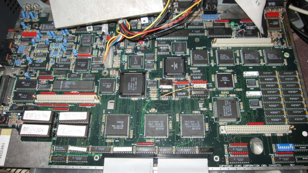
C302406-001
This section will be much shorter as I inevitably had to cover a lot of it in the previous sections. But here are a couple of board shots:
REV.H:
And a REV.J
Notice the lack of wires on the bottom part of the board, unlike the previous REV D models. I do not have any pictures of a REV K but I would assume that it would probably have the same rework on it as we see in these two as I explained in the previous section, I doubt that Atari would make another FAB REV to fix the changes.
REV A
Eh? We're back to this now? Time for a refresher. We're talking about the FAB and its revision:


I believe this to be the only revision of the C302406-001 FAB and as such, the very last TT board. I base this simply on the manufacturing dates shown above. We are well into 1992 at this point and Atari was starting to focus whatever little interest it had left on computers on the Falcon. And we know that it waned quite dramatically where Atari all but abandoned the Falcon and the computer line to go all-in on the Jaguar.
We also haven't heard of any later revisions than REV.K and most of what I know of them is from Simbo's observations having worked on several of them.
Again, I'd like to be proven wrong so please send me pictures of boards that are not included here.
Schematics
I'm inserting this part here as it has severe implications to the sections ahead. There are no known schematics for this FAB. I don't even have to prove that as both known schematics clearly indicate they are for C301763-001 and dated much earlier than these to REV.H models. You can verify this yourself by locating U402 next to the battery. It is the IC that gets removed in the RTC Fix. All boards prior to this need the chip to be removed. Since this FAB never had this chip, it's safe to assume that it would also not appear in the schematic. Just like we saw with the subtle differences between the two schematics from the same FAB earlier.
Also, Simbo confirms this rather emphatically here:
best is holding out becouse prob knowone bought it from him schematic for rev J would be an orgasim for sure
i think this is a needed mos for h- j-k
like me
ill stick on some cash if some people want to go share
for the schematics for rev j
share on a board fund basis
if it takes payin a couple of homboys to go around
then so be it...
So the implications of not having schematics are that we cannot rely 100% on current schematics meant for another FAB as even within a FAB there can be changes. We can overcome this by being careful and logical.
The other problem is that we don't have a listing of revisions and the ECOs to get there as with the REV D-G.
Let's still cover the ASSY revisions then the best that we can, starting with:
REV.H
I like to include a period between REV and the letter so as to distinguish it from the FAB revision. Well, we have plenty of pictures of this particular board leading me to believe that this is likely the most sold version of the SMD models, if not the entire line.
If REV G was the last of the C301763-001, this being H must be the first of the C302406-001. And since we have two examples of C302406-001 REV A being REV.H we can 100% trust this.
With all this evidence, we have no choice but to accept, that the other REV.H is an upgraded REV D. And because none of the REV A REV.H models have the patches on the bottom of the board we have to conclude that if ECO# 1323, which is part of that wiring, upgrades to REV G, that only leaves one possible outcome. REV.H is achieved through the VME Bus Fix. If only that rework guide could have had the ECO# or date.
This will help. Here is the last known Atari Technical Bulletin TT30-0007:
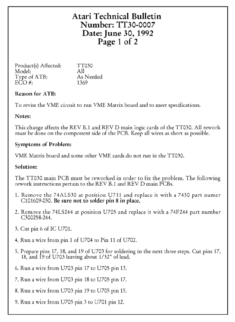
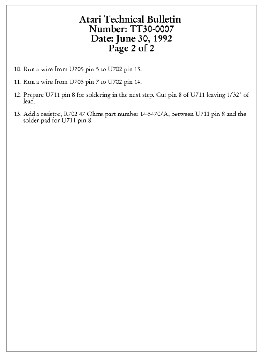
Looking at the date above, we're well past the manufacturing dates of the C302406-001 REV A-boards. Also, this fix is meant for REV B1 & REV D boards that we now know without a doubt to be C301763-001 FABs. This confirms my conclusions that REV.H and later boards, or in other words all C302406-001 boards have this fix and all pre ECO #1369 patches. This also confirms that B1 PGA boards can attain this prestigious level.
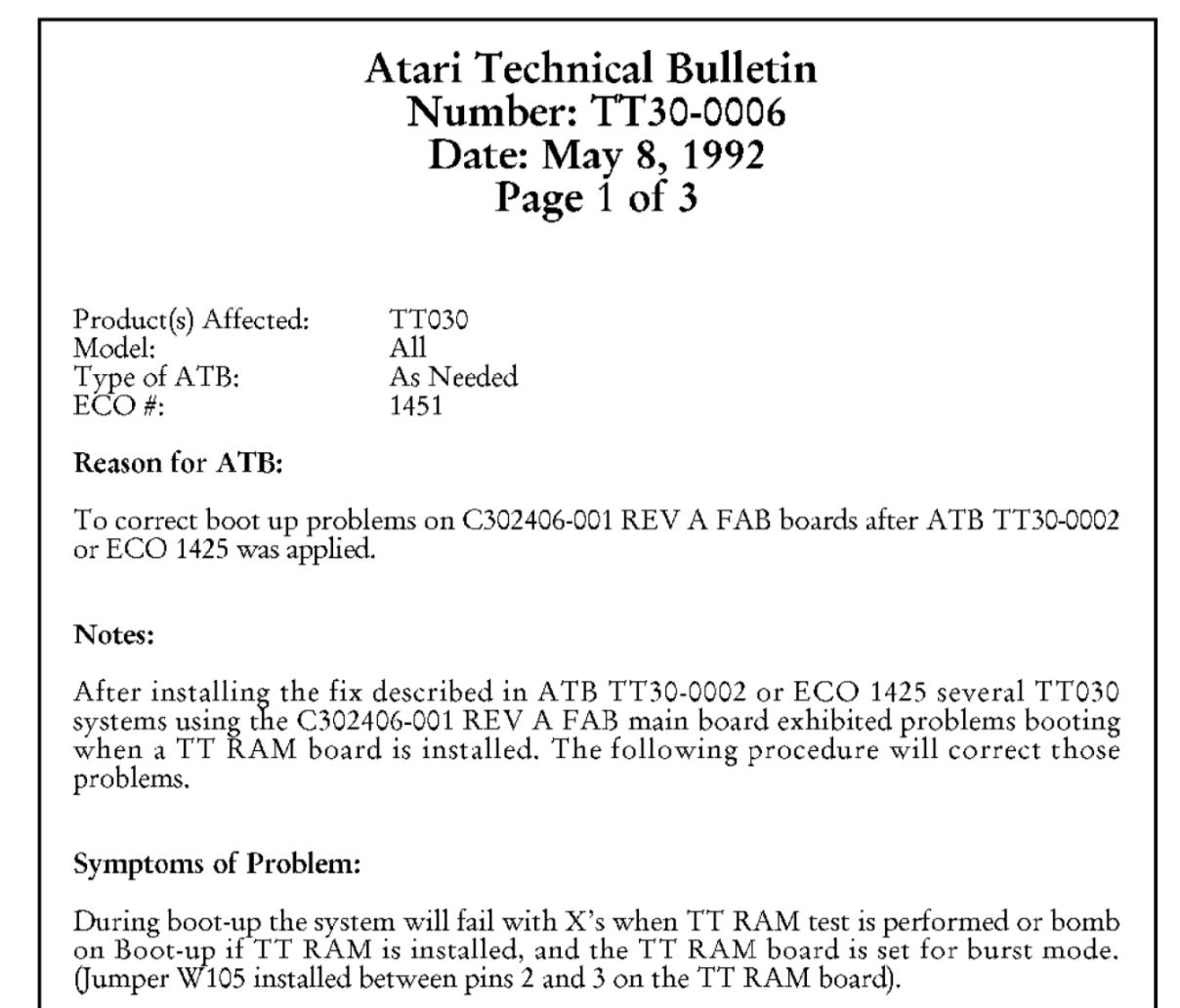
What about the patches that we do see on C302406-001 boards? Those appear on earlier Atari Technical Bulletins. Most likely it is either TT30-0006 or TT30-0002 that 0006 was supposed to fix:
This variant of the fix is outlined and illustrated in my Atari TT030 REV.D Rework Guide.
REV.J
Never seen or heard of REV.I, so we move to REV.J. And that's all I have to say about REV.J.
REV.K
Seriously, I had nothing on J. REV.K on the other hand is supposedly the very last TT. As I mentioned earlier, I doubt that REV.K is free of rework. If it were, it would mean that it would be C302406-001 REV B or something and I find that highly unlikely due to reasons already stated. I think it's simply a small fix that got applied after REV.J's fixes.
How about the REV.K board settings schematics floating around? It doesn't seem to pertain to this REV.K. The date is wrong, the ASSY is wrong and, quite frankly, even if they were correct, it gives absolutely no helpful information. I'm not even going to post a picture of it.
Conclusion
So, just like my 1-month summer vacation is about to, we have reached the end of this saga. What to call your C302406-001?
The Last Revision of the TT is fine
C302406-001 REV X is great
Don't call it REV.H without clarifying whether it's C301463-001 REV D or C302406-001 REV A
REV.J or REV.K is fine as there is no room for interpretation there.
Final Words
If you managed to read this far, congratulations, you deserve a/your TT. Treat it well.
As to what to call the revisions, my opinion is that we primarily use ASSY REVs as they are the single most consistent naming scheme. Here are my suggestions:
REV.A - First model, C300720-001, 16Mhz or 32Mhz with daughterboard
REV.B - Second model, C300720-001, 32Mhz with daughterboard
REV.C - PGA model, C301763-001 REV A & B1 (if you actually happen to have REV.E or REV.F give them in conjunction with REV.C)
REV D + ASSY REV - first SMD model, C301763-001 REV D (example REV D upgraded to REV.G or REV.H)
REV.H, Latest FAB - C302406-001 REV A
REV.J
REV.K
If you have more information, suggestions or corrections, contact info is on the bottom of the page. Or you can reply to the threads that this gets posted to. I will update this guide as needed. When enough time had passed, I will compile a PDF of it.