
I thought I'd post pictures of my latest restoration project as I realized I had never done that . Unlike my previous projects, this was a "restored to order" job with some specific requests.
This was the starting point. A little dirty but not bad at all.

Here is the motherboard before any work has been done. Very clean. It's the last revision of the small STs and only one that supports 2-chip TOS.
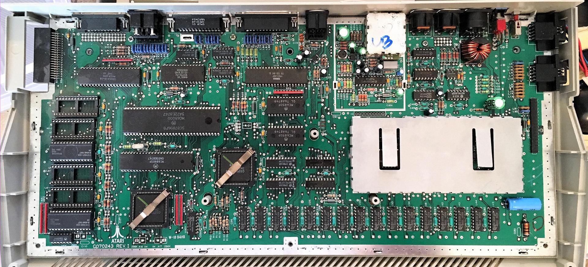
Right off the bat I noticed that there has been minor rework on the board. It's clear that a bunch of resistors have been changed. They are connected to the RAM chips and the MMU (memory management unit). It seems that someone wanted 68ohm resistors instead of the original 33ohms. Marked in yellow. No idea why it was done and no reason to. I decided to revert to 33ohms.

The first specific request was for 1MB ram instead of the 512KB from factory. I chose to upgrade using the same method Atari used on the 520+, which was the piggyback method. I took some old 256KB-simms with suitable 41256 chips and removed 16 chips that I then proceeded to solder on top of the 16 ram chips on the motherboard leaving pins 4 and 15 free to run wires. For more details see this thread on atari-forum.com.


I left wires long at this point. This board revision had nice locations for the wires. I installed 68ohm resistors and cut the bridge on the other side on RAS1.

Here I reverted back to the original 33ohm resistors. Notice the fruit of my OCD with the stripe alignments. This was worth doing just because this previous change was a botch job. The original resistors had been snipped off instead of properly de-soldered and crazy amounts of solder was used. It was really crusty.

Here's a post op picture of the solder side of the same location. The solder mask was quite fragile so I applied solder mask where needed and cured it with UV.

Here's a shot of a cleaned top case. I always remove the badge as it's very susceptible to damage. I also always spray a few coats of matte lacquer on it to give it some protection.

The second specific request was for a dual TOS. There was to be no visible switch either. I had to hack a solution as I had a deadline to keep. Here is the result. I used two 27C020 chips. I'm picking VCC of the neighbouring sockets because A17 (pin 30) is obscuring VCC on pin 28 of socket. Likewise it's easier to pick A16 from pin 22 of neighbouring socket rather than routing it awkwardly under the chip. Then GND is connected to OE. A17 is pulled low by 10K resistor when jumper is off. That's one TOS version. Putting in the jumper pulls A17 to +5v and another TOS is selected. Not pretty but it works. I made a point of not soldering anything on the board in case the roms got changed.


Here we have all board work complete. I changed all the caps and pull-up resistors for the address lines to 3.3K ohms. All circled below.

Underside completed. Reflowed most of the connection. Applied soldermask where needed and then a thorough cleanup.

Like new. Keycaps are double-shot so very durable and you can't erase the legends. Note the different shade loose key. I've encountered at least three different shades of keycaps.

Finished product. Picture doesn't do it justice.

For all this, the customer paid $140 + shipping.